23 Sep 2010-24 Sep 2010|Noida | Amity University Campus, Sector-125 Noida
Amity School of Engineering & Technology organises Two Day National Conference (VMN 2010 ) - On ‘Very Large Scale Integrated Circuit (VSI)’, ‘Micro Electronics Mechanics (MEMS) & Nano Electronic Mechanics (NEMS)

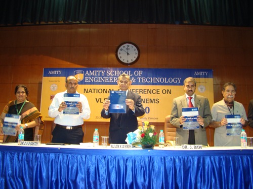
Amity School of Engineering (ASET) organized the first two day National Conference on “VLSI, MEMS and NEMS” (VMN’ 2010) on September 23-24, 2010 at ASET, Amity University Campus, Sector – 125, Noida.
The technical conference aimed at providing a platform for industry, academia and students regarding advancements in research and development in “VLSI, MEMS and NEMS” and its related fields. “VMN 2010” focused on bringing together professionals, students, enthusiasts to discuss various emerging trends, innovation, share research results and new directions in the field of VLSI Technology, MEMS and NEMS.
Inaugurating the conference Dr. C V S Sastry, Director – ANURAG and DRDO, expressed his pleasure and honor on being at the occasion of first National Conference on “VLSI, MEMS and NEMS” and said “Amity University is reputed to be the best university in private sector in India with several firsts to its credit such as first wireless campus. The founders of Amity have established this University as a think tank for higher education & research and to prepare the youngsters to be creative, innovative thinkers and nation building entrepreneurs. Investment in these institutes advances knowledge through education in research in such manner that students will be of service to the community and nation.” Dr. Sastry apprised the audience about “Sytem Design Trends (Programmability in design, Design at an abstract level & Sstem design verification / validation)”, “Electronic system- level (ESL)” and “Register- transfer level (RTL) implementation”. He advised the students that “they need to bridge the gap in their ability of architecturing and testing to be able to do the entire sytem design themselves. There is a requirement to seek and creat opportunities to complete chip design, based on specification of an intended design, engineers implement timing critical components like CPUs or functional critical analog components as hard macros. We need domain specific design strength. The risk aversion mind set needs to be changed particularly among high-tech professionals. Building critical IPs such as India Processor, driven by national pride, security of market potential must be essential.” He urged that there is a need to identify India Specific products in the fields of e- learning, e- governance and tele- medicine.
Dr. J. Daw, Managing Director Mentor Graphics India, shared several ideas on “VLSI Design”, “Impact and future of VLSI (Business impact and Social impact)” and “Structure and relevance of the semi conductor market”. Dr. Jaw laid emphasis on the “Contribution of MEMS towards technological cost reduction today” and “Micro processors”. Dr. Daw strongly recommended higher education for the students in order to nurture intellectual property and said “students must have their hands on silicon in the laboratories.”
Welcoming the honorable guests and dignitaries, Dr. Balvinder Shukla, Pro Vice Chancellor (A), Director General ASET, shared ideas on “VLSI- electronic design automation” and “the move from VLSI to MEMS and its usefulness in the telecommunication industry”. Dr. Shukla expressed deep interest in strengthening the association of Amity and Mentor Graphics.
Wishing success to VMN 2010, Maj. Gen K. Jai Singh, Vice Chancellor, Amity University Uttar Pradesh, said “It is a great learning experience over two days at VMN 2010.”
The conference was followed by a Plenary Session by Dr. M.J Zarabi, Ex- CMD, SCL. “Thin Gate Dielectrics in Sub-100nm devices- How they behave?” by Dr. M.K Radhakrishnan, Nano Rel, “How VLSI design will be a future?” by Mr. Jaswinder S. Ahuja, Cadence, “Problems and Pittfalls in Low Power VSLI Design”, by Dr. Subir K. Sarkar, Jadavpur University, “Applications of Micro and Nano technologies” by Dr. V.K Jain, AIAERS. Technical sessions on “Micromachined Microwave and Millimeter Wave Circuit Design” by Dr. Shiban K Koul, IIT Delhi, “Role of Emerging Technologies in Semiconductor and Overall Electronic Industry” by Mr. Hitesh Garg, NXP Technologies, “Functional Materials” by Dr. k.L Yadav, IIT Roorkee, “Opportunities in Emerging Technology Market”, by Mr. Rajendra Pratap, Cadence and “Molecular Logic Array and Memory Devices in Technology” by Mr. Suresh Janagam and Mr. M. Ramesh were held.
Technical sessions on “Fabrication & Characteristics of Zno NEMS-Device”, by Prof. P. Chakrabarti, IT- BHU, “A New Fabrication Process for RF- MEMS Switches in CPW Configuration on Glass Substrates” by Dr. Amitaba Das Gupta, IIT Madras, “Design and Implementation of Micro-machined Cantilever Structure for MEMS Based Digital Inverter”, by Prof. T.K Bhattacharya, IIT Kharagpur, “ Junction Less Field Effect Transistor, by Prof. R.S Gupta, University of Delhi and “VLSI Interconnects” by Dr. B. Kaushik, IIT Roorkee will be held tomorrow.
Also present in the conference were Maj. Gen R.K Dhawan, Senior Vice President, Amity International Affairs Division, Prof. V.K Jain, Director, Amity Institute of Advanced Research & Studies, Prof. K.M Soni, HOD E& CE, faculty members of ASET, dignitaries and students.